|
|
|
|
中文版 | News | Archives | Reviews | Forum | $ Deals | Links | History | Contact | Privacy |
|
| ||||
|
Chaintech 7NJS nForce2 Mainboard Gallery (2)
The second nForce2 board arrives today (Sunday) in our labs. Although it is a sunday and it is a public holiday tomorrow, I decided to take a few snapshots of the package and do a overclocking test of the board. The detail review will come later. The Mainboard
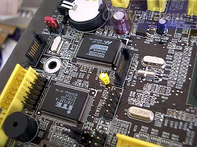
On the left is the floppy connector. The Promise PDC20376 SerialATA controller supports two serial ATA ports and one UDMA 100/133 IDE port with RAID 0/1. Another two standard ATA133 IDE interface connects up to 4 IDE devices.
3 DIMM slots supporting up to 3G. Dual Channel DDR400 is supported. To enable Dual Channel, one DIMM must be inserted into DIMM 3 (independent dimm slot) and the other can be in DIMM 1 or 2.
4 mounting holes around CPU socket A. Does the heatsink looks cool? There is a jumper JP25 that sets default 100 or 133/166 default CPU FSB
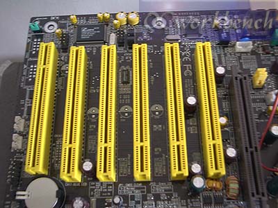
1 ACT, 5 PCI, 1 AGP slot. 6 channel audio is provided by CMedia 8738 chipset
Another view of the 2 SATA connectors on board
Back Panel of Mainboard. One LAN port only.
|
|
(C) Copyright 1998-2009 OCWorkbench.com
|